{{serverconnectlatestnews.data.showlatestnews.data[0].news_title}}
{{serverconnectlatestnews.data.showlatestnews.data[0].news_date.formatDate("d MMM yyyy")}}
{{serverconnectlatestnews.data.showlatestnews.data[0].news_teaser}}

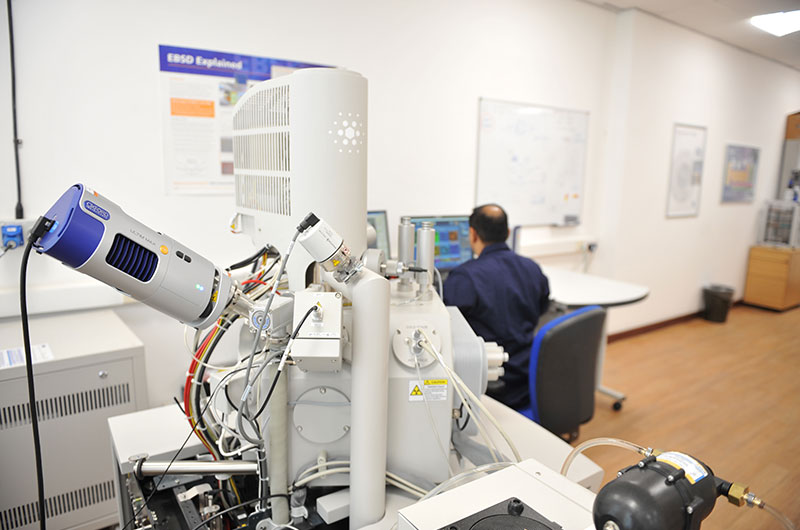
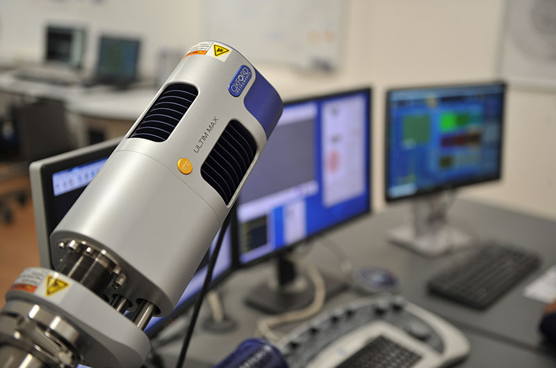
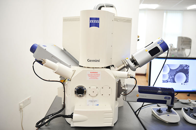
Scanning electron microscopy (SEM) is an analysis technique which obtains information about composition and topography of an object by scanning its surface to create a high-resolution image.
SEM uses a focused beam of electrons to do this. The resulting images show information about what the object is made of and its physical features. SEM has a broad range of applications, across several industries and sectors.
These scanning electron microscopes are complimented with the latest technology, including:
FEI Quanta 650 w/Scanning Electron Microscope
Zeis Sigma 300 w/Scanning Electron Microscope
Enquire about services, facilities, and expertise.
Materials Processing Institute is registered in England with registered No. 08919614
Registered Office: Materials Processing Institute, Eston Road, Middlesbrough TS6 6US
© Copyright Materials Processing Institute
Terms & Conditions / Terms & Conditions of Metal Sales / Website Terms & Conditions / Privacy Policy / Cookies Policy / Data Protection Notice / Site Map
Website by VIA Creative