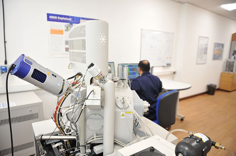
Capability Update - Scanning Electron Microscopy

Scanning Electron Microscopy (SEM) is an analysis technique to get information about composition and topography of an object by scanning its surface to create a high-resolution image.
◾ SEM provides detailed, magnified images of surfaces, allowing researchers to observe structures and features that are invisible to the naked eye or traditional light microscopy.
◾ SEM generates three-dimensional images, providing a depth of field that allows for the study of complex structures.
◾ SEM can be combined with energy-dispersive X-ray spectroscopy (EDS) to identify the elemental composition of a sample, providing valuable information about its chemical makeup.
◾ SEM is used in quality control processes and research studies to analyse the microstructure, morphology, and composition of materials.
Here are more details about out our range of high-resolution Field Emission Scanning Electron Microscopes (FE-SEM) complimented with the latest technology, including:
◾ Wavelength Dispersive Spectroscopy (WDS) and
◾ Electron Diffraction Spectroscopy (EDS) detectors offering light element analysis
◾ Electron Back-scatter Diffraction (EBSD)
◾ Environmental Scanning Electron Microscopy (ESEM)
Link to more information - https://www.mpiuk.com/equipment-scanning-electron-microscopy.htm
11 June 2025


